все чудово, плата працює коректно

 , потім у швидкість повітря
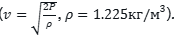 .
.

Оксана Д.
Переможець
37
0
- Проєкти 36
- Оцінка 5.0
- Рейтинг 1 410
Бюджет: 2000 UAH Термін: 10 днів
Добрий день. Можу зробити схему і плату в Altium Designer або Kicad.
Скопіювати
26 березня 2025

Ставки поки відсутні
Фрилансери знайомляться з завданням — скоро тут з'являться пропозиції.
Ставки приховані
У списку не показані ставки, приховані замовником чи фрилансером з Plus, а також ставки, що порушують правила
-
 Rostislav G.
 25 березня 2025
Прошивка є, потрібна тільки схемотехніка та розведення плати
-
Rostislav G.
25 березня 2025
Components
- U1: AMS1117-3.3 (3.3V regulator)
- U2: MPXV7002DP (airspeed sensor)
- U3: STM32F103C8T6 (microcontroller)
- U4: MCP2551 (CAN transceiver)
- C1: 10 µF (regulator input capacitor)
- C2, C3, C4: 0.1 µF (decoupling/filter capacitors)
- R1: 1 kΩ (ADC protection resistor)
- R2, R3: 4.7 kΩ (I2C pull-ups)
- R4: 10 kΩ (MCP2551 RS resistor)
- R5: 120 Ω (optional CAN termination)
- J1: 2-pin header (5V power input)
- J2: 4-pin SWD header (programming)
- J3: 4-pin JST-GH (DroneCAN output)
- J4: 4-pin header (I2C output)
Connections- Power Input (J1):
- Pin 1: 5V from drone BEC
- Pin 2: GND
- 5V to U1 Pin 1 (IN), C1 (10 µF) between Pin 1 and GND
- Regulator (U1 - AMS1117-3.3):
- Pin 1 (IN): 5V from J1
- Pin 2 (GND): GND
- Pin 3 (OUT): 3.3V
- C2 (0.1 µF) between Pin 3 and GND
- Airspeed Sensor (U2 - MPXV7002DP):
- Pin 1 (GND): GND
- Pin 2 (Vout): To R1 (1 kΩ), then U3 Pin 23 (PA0), with C3 (0.1 µF) from R1-PA0 junction to GND
- Pin 3 (Vcc): 3.3V from U1
- Pin 4 (NC): Not connected
- Microcontroller (U3 - STM32F103C8T6):
- Power:
- Pin 9 (VDD): 3.3V
- Pin 8 (VSS): GND
- C4 (0.1 µF) between Pin 9 and Pin 8
- ADC:
- Pin 23 (PA0): From U2 Vout via R1
- I2C:
- Pin 20 (PB6): SCL to J4 Pin 1, R2 (4.7 kΩ) to 3.3V
- Pin 21 (PB7): SDA to J4 Pin 2, R3 (4.7 kΩ) to 3.3V
- CAN:
- Pin 33 (PA11): CAN_RX to U4 Pin 4
- Pin 34 (PA12): CAN_TX to U4 Pin 1
- SWD (Programming):
- Pin 34 (PA13): SWDIO to J2 Pin 1
- Pin 35 (PA14): SWCLK to J2 Pin 2
- J2 Pin 3: 3.3V
- J2 Pin 4: GND
- CAN Transceiver (U4 - MCP2551):
- Pin 1 (TXD): U3 Pin 34 (PA12)
- Pin 2 (VSS): GND
- Pin 3 (VDD): 3.3V
- Pin 4 (RXD): U3 Pin 33 (PA11)
- Pin 6 (CANL): J3 Pin 2
- Pin 7 (CANH): J3 Pin 1
- Pin 8 (RS): R4 (10 kΩ) to GND
- J3 (DroneCAN):
- Pin 1: CANH
- Pin 2: CANL
- Pin 3: 5V (passthrough from J1)
- Pin 4: GND
- R5 (120 Ω) optional between J3 Pin 1 and Pin 2 (if bus end)
- I2C Output (J4):
- Pin 1: SCL (U3 PB6)
- Pin 2: SDA (U3 PB7)
- Pin 3: 3.3V
- Pin 4: GND
-
 Олексій Мамонтов 26 березня 2025
MPXV7002 (працює при 2.7-5.5 В, тому 3.3В підходить

Даташит про це не в курсі )
-
Олексій Мамонтов 26 березня 2025
https://static6.arrow.com/aropdfconversion/12aa4fe8022de2ea70f9cf3b6991e13f4191d250/mpxv7002.pdf
-
Rostislav G.
27 березня 2025
Step 1: Place Components
- Open the Library:
- In EasyEDA, go to the left panel and click Libraries > Search.
- Place Each Component:
- Search for each part by its Supplier Part (LCSC part number) or Manufacturer Part. If the exact part isn’t found, use a generic equivalent and update the part number later for PCB ordering.
- Place and label each component as follows:
- J1 (Power Input): Search HDR-F-2.54_1x2 or C124404. Place it, label as J1.
- U1 (Regulator): Search AMS1117-3.3 or C84062. Place it, label as U1.
- U2 (Sensor): Search MPXV7002DP or C512345. If not found, use a generic DIP-4 symbol (4-pin DIP package) and label as U2.
- U3 (MCU): Search STM32F103C8T6 or C111293. Place it, label as U3.
- U4 (CAN Transceiver): Search MCP2551-I/SN or C14671. Place it, label as U4.
- J2 (SWD): Search HDR-F-2.54_1x2 or C124404. Place it, label as J2.
- J3 (CAN): Search HDR-F-2.54_1x2 or C124404. Place it, label as J3.
- J4 (I2C): Search JST-GH-4 or C165050. Place it, label as J4.
- R1, R5 (10kΩ): Search 10k or C25804. Use an 0805 resistor symbol, place two, label as R1 and R5.
- R2, R3 (4.7kΩ): Search 4.7k or C25802. Use an 0805 resistor symbol, place two, label as R2 and R3.
- R4 (120Ω): Search 120R or C25744. Use an 0805 resistor symbol, place one, label as R4.
- C1, C2 (10µF): Search 10uF or C92442. Use an 0805 capacitor symbol, place two, label as C1 and C2.
- C3, C4 (100nF): Search 100nF or C14663. Use an 0805 capacitor symbol, place two, label as C3 and C4.
- Position Roughly:
- Place J1 on the left side (power input).
- U1 (AMS1117-3.3) to the right of J1.
- U2 (MPXV7002DP) below U1.
- U3 (STM32F103C8T6) in the center.
- U4 (MCP2551) to the right of U3.
- J2, J3, J4 on the right side (for SWD, CAN, I2C).
- Passives (R1-R5, C1-C4) near their respective components (e.g., C1 near J1, R1 near U2).
Step 2: Connect WiresUse the wire tool (W key) to connect the components based on the original JSON’s shape array. You don’t need to match the exact coordinates—just connect the correct pins. Here’s the wiring list:- Power and Ground:
- 5V: J1-1 to U1-IN.
- GND: J1-2 to U1-GND.
- 3V3: U1-OUT to U2-Vcc.
- 3V3: U1-OUT to U3-VDD_1 (pin 24).
- GND: U1-GND to U2-GND.
- GND: U1-GND to U3-VSS_1 (pin 23).
- 3V3: U1-OUT to U4-VCC.
- GND: U1-GND to U4-GND.
- 3V3: U1-OUT to J4-3.
- GND: U1-GND to J4-4.
- Sensor to MCU:
- Vout: U2-Vout (pin 2) to R1-1.
- ADC_IN: R1-2 to U3-PA0 (pin 10).
- CAN Interface:
- CAN_TX: U3-PA12 (pin 33) to U4-TXD.
- CAN_RX: U3-PA11 (pin 32) to U4-RXD.
- CANH: U4-CANH to J3-1.
- CANL: U4-CANL to J3-2.
- I2C Interface:
- SCL: U3-PB6 (pin 42) to J4-1.
- SDA: U3-PB7 (pin 43) to J4-2.
- SWD Interface:
- SWDIO: U3-PA13 (pin 34) to J2-1.
- SWCLK: U3-PA14 (pin 37) to J2-2.
- Passives:
- C1: Between J1-1 (5V) and J1-2 (GND).
- C2: Between U1-OUT (3V3) and U1-GND.
- C3: Between U3-VDD_1 (pin 24) and U3-VSS_1 (pin 23).
- C4: Between U4-VCC and U4-GND.
- R2: Between J4-1 (SCL) and J4-3 (3V3).
- R3: Between J4-2 (SDA) and J4-3 (3V3).
- R4: Between J3-1 (CANH) and J3-2 (CANL).
- R5: Between U3-BOOT0 (pin not specified in JSON, typically pin 44) and GND (connect to U3-VSS_1).
Step 3: Verify and Tidy Up- Check Nets: Hover over wires to confirm net labels (e.g., 5V, GND, ADC_IN, CANH, SCL).
- Adjust Layout: Drag components and wires to make the schematic readable. Aim for a logical flow (power on the left, MCU in the center, interfaces on the right).
- Add Annotations: If needed, add text labels (e.g., 5V, 3V3) using the text tool (T key).
Step 4: Convert to PCB- Once the schematic is complete, go to Design > Convert to PCB.
- The PCB will be ~25x20mm, and the total cost is ~$16.12 (still under $20).
- I can help with PCB layout if needed—place U3 in the center, U1/U2/U4 around it, connectors on the edges, and passives in between.
Актуальні фриланс-проєкти в категорії Вбудовані системи та мікроконтролери
-
5000 UAH
Мала обертальна дротова камера
3 ставки 29 липня
-
Не вказано
Розробка та доопрацювання PCB на основі наявного макету
Машино- та приладобудування 4 ставки 28 липня
- Не вказано
Завантаження...
Завантаження...